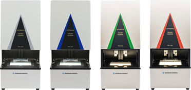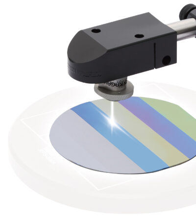


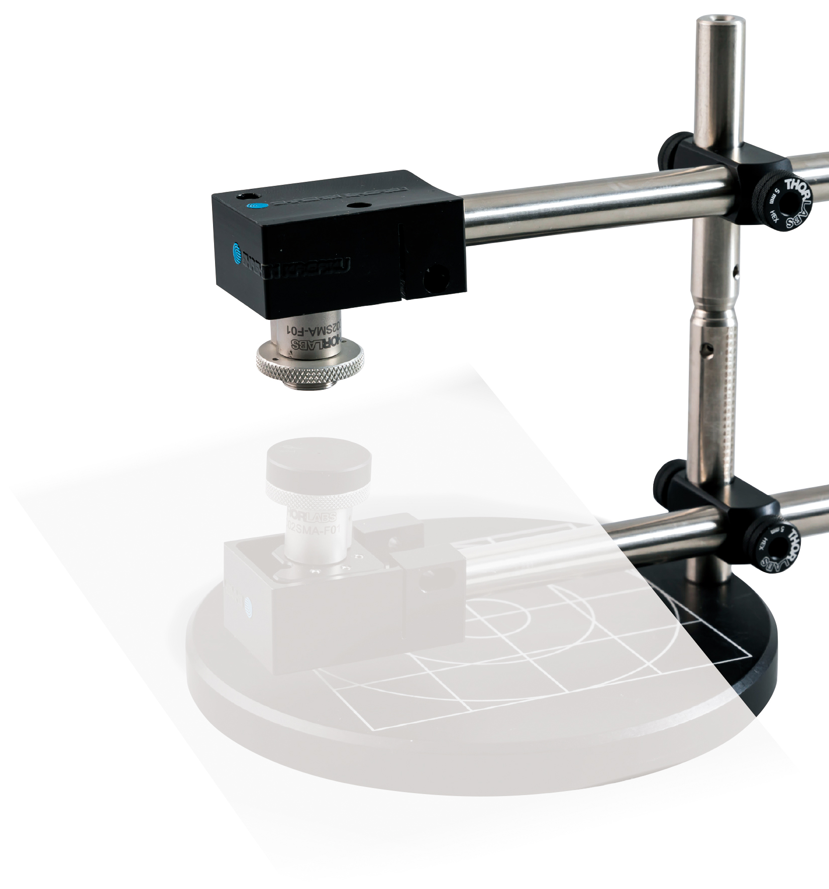

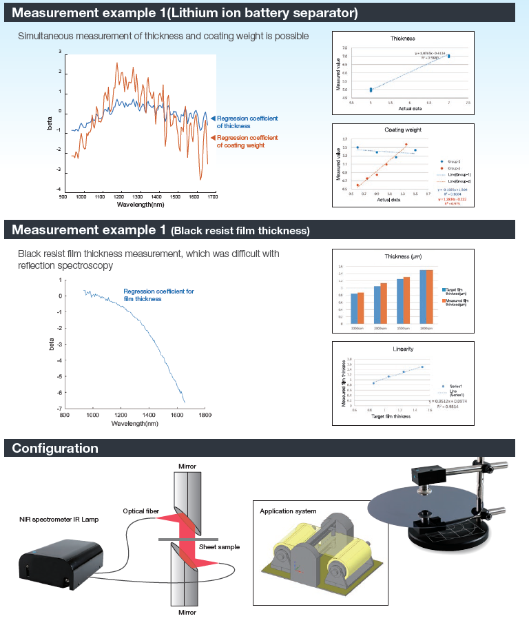
Infrared Sheet Thickness Monitors: Versatile for measuring battery separators, coatings, and silicon, suitable for lab and in-line production inspections.Infrared sheet thickness monitors measure the thickness of translucent sheets such as battery separators, low reflective coatings such as black resist, and silicon. It can be used in all applications from laboratory level to in-line 100% inspection in production. The infrared absorption system consists of a compact mirror probe with a transmissive optical system, which allows simultaneous measurement of multiple parameters such as film thickness, density, and composition at more than 100 wavelengths.
1.Measures the thickness of translucent sheets, low-reflection films, silicon, etc., which was difficult with the optical interferometry 2. Compact probe
Adopting a small 30 mm reflective probe, it can be installed in a small space in equipment or production lines. In addition, since the probe is connected to the main body only with an optical fiber cable, it has excellent environmental resistance.
3. High-speed measurement Simultaneous sampling of near-infrared wavelengths from 950 nm to 1600 nm at 100 points or moreIt enables rapid sampling with min 1mm sec. It enables measurement on the production line on a real-time basis. It is superior for durability and consistency due to nonimpact filter use.
4. Thickness measurement reproducibility 0.1% or less (3σ) 5. Measurement algorithms| Algorithm | Calibration sample | Number of parameters |
| Lambert-Beer law | 1 | Thickness |
| The least squares regression method | 2 or more | Multiple parameters (Thickness, Density, Composite ratio, etc.) |
Related Products
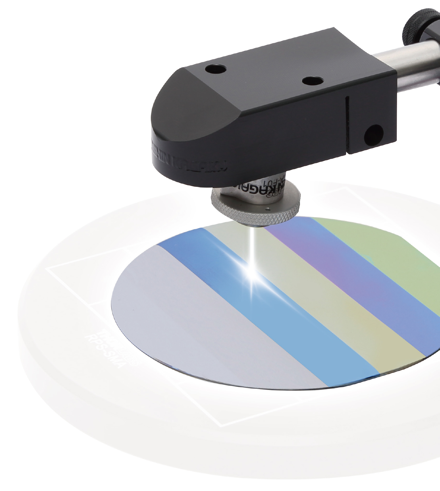 Compact Flim Thickness Reflection spectrophotometric meter for laboratory to in-line inspection, measuring up to 9 transparent films simultaneously.
 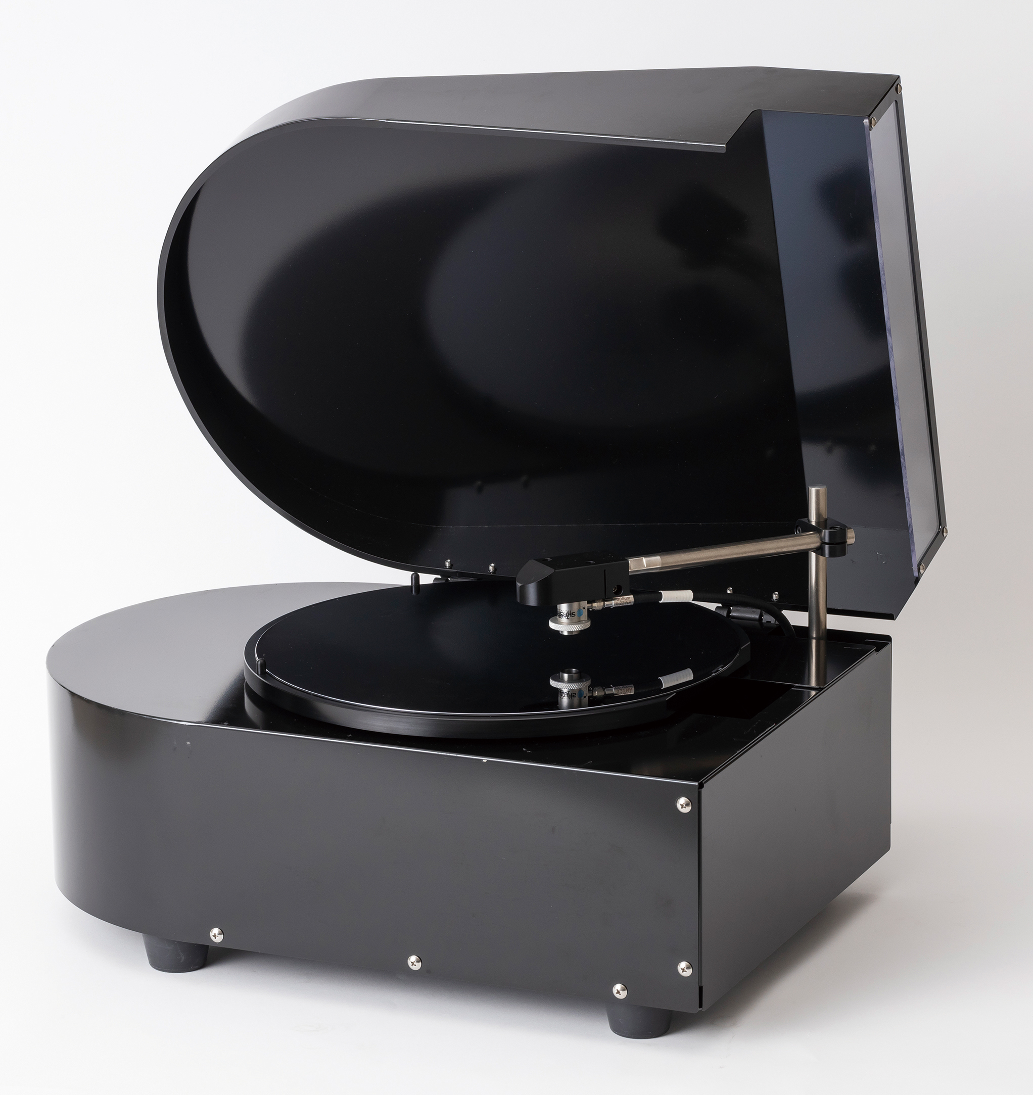 Automatic wafer Mapping Device Reliable film thickness mapping for up to 300 mm wafers, ideal for semiconductor manufacturing with self-calibration and cleanliness.
| Cup size | Maximum 1kg (Gross Weight)x 2cups |
|---|---|
| Other containers | Multiple containers and syringes can be used by using an adapter. |
| Speed of revolution | Settable in 9 steps |
| Speed of rotation | Settable in 10 steps |
| Settable time | Maximum 990 seconds (5 Step total) |
| Step mode | 5 steps Continuous operation with 5 different operation patterns (condition settings) is possible |
| Memory channel (condition setting memory) User settable channels Fixed data channels | 90 10 |
| Power supply voltage | Single phase AC 200-240VAC 50/60Hz |
| Power consumption | 2.0kW |
| External dimensions | W565 × D597 × H741(㎜) |
| Main unit weight | Approx. 140kg |